Semiconductor manufacturing requires extreme precision and reliability, as even minor imperfections can impact device performance. Welding is a crucial process in ensuring the durability of semiconductor components, from wafer fabrication to packaging. Advanced techniques like laser welding and electron beam welding (EBW) offer high precision, minimal heat input, and contamination-free joints. This article explores the best semiconductor welding methods, their applications, and the challenges involved in ensuring durability.
Laser Welding
Laser welding is widely used in semiconductor manufacturing because of its non-contact nature, high precision, and ability to weld delicate materials with minimal heat damage. Key advantages include:
- Micron-level accuracy – Essential for microelectronic components with intricate geometries.
- Minimal thermal impact – Prevents damage to heat-sensitive semiconductor materials.
- Clean, high-purity welds – No need for filler materials, reducing contamination risks.
Common applications of laser welding in semiconductors include hermetic sealing of microchip packages, sensor assembly, and bonding delicate electronic components.
Electron Beam Welding (EBW)
Electron beam welding is another critical method in semiconductor manufacturing, particularly for applications requiring deep penetration, high-purity welds, and precision bonding. Advantages of EBW include:
- Weld depths up to 2 inches – Ideal for applications requiring deep, strong joints.
- Extremely clean welds – The vacuum environment eliminates oxides and contaminants.
- Minimal distortion – The small heat-affected zone (HAZ) ensures precision in microelectronics.
EBW is commonly used for joining semiconductor enclosures, assembling microelectronic circuits, and welding high-performance electronic components in aerospace and defense applications.
 |
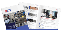
GuideElectron Beam Welding Essentials Guide |
Applications of Semiconductor Welding
Welding enhances durability and performance in various semiconductor applications, including:
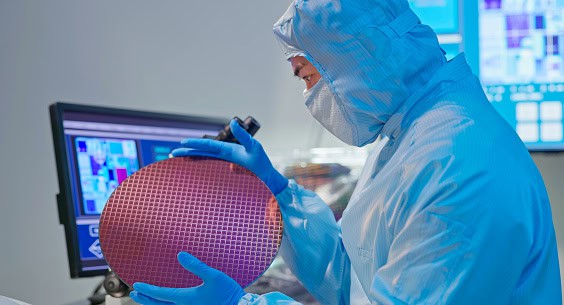
- Semiconductor wafers – Electron beam welding ensures high-strength, reliable bonding of wafer components.

- Microchip packaging – EBW and laser welding provide hermetic seals, protecting delicate microelectronics from contaminants.
- Optoelectronic devices – Welding secures connections in fiber optics, sensors, and RF/microwave components.
Challenges in Semiconductor Welding
Despite its advantages, semiconductor welding presents several challenges:
- Heat Control – Both laser and electron beam welding require precise heat management to avoid damaging fragile semiconductor structures.
- Micron-Level Precision – Semiconductor components often require welds at the sub-micron level, necessitating highly specialized CNC-controlled welding equipment.
- Material Compatibility – Some semiconductor materials, such as highly reflective metals like aluminum and copper, require optimized welding parameters to prevent cracking or oxidation.
 |
WebinarWelding 101 Precision Welding Tips for Electron Beam, Laser Welding and Laser Hermetic Sealing |
Welding for Long-Lasting Microelectronics
Semiconductor welding is vital for enhancing the reliability, strength, and longevity of microelectronic devices. Laser welding and electron beam welding provide precision, cleanliness, and high-performance bonds, making them essential in semiconductor manufacturing. As technology advances, continued innovation in welding techniques will ensure the durability of next-generation semiconductors.

